Skip to content
    Industries

    BIM/VDC for Semiconductor & Cleanroom Facilities

    Contactless scanning protocols for active fabs. ISO cleanroom-compliant workflows. Tool installs and process bay retrofits documented to fab tolerances.
    Industry context

    Why it matters

    ISO 5
    Cleanroom protocols supported

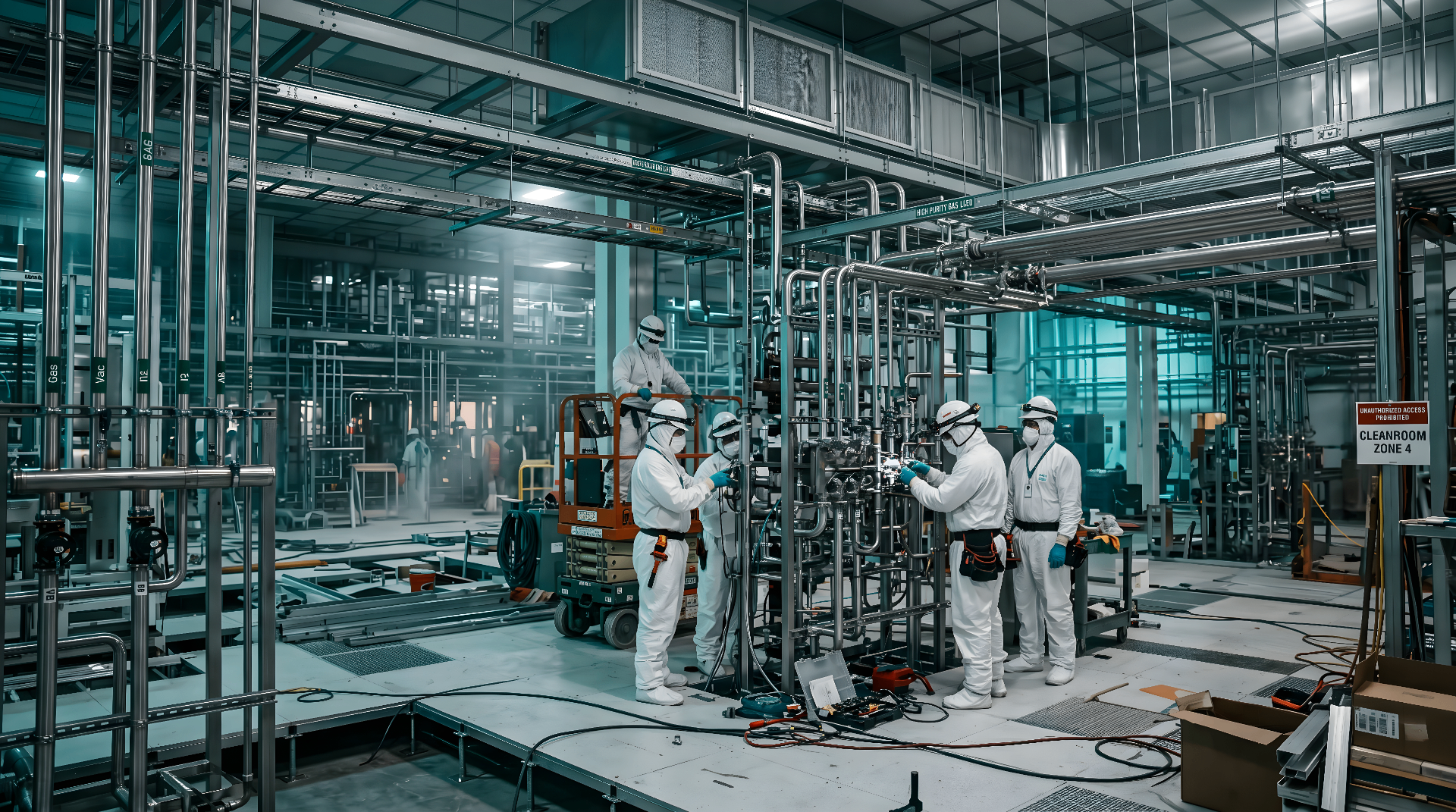
    Semiconductor fabs are the most demanding scanning environments in the industry. Cleanroom protocols, vibration sensitivity, EHS oversight, and tool install schedules leave zero room for documentation error or operational disruption. Most scanning vendors have never set foot in a fab.

    We've built fab-specific protocols from the ground up: contactless scanning that respects ISO Class 5 and below environments, gowning and equipment decontamination procedures, EHS coordination for active process areas, and field crews trained on fab-specific safety and access requirements.

    Engagement scope

    What we deliver

    A defined deliverable package — scoped, fixed-fee, and documented for semiconductor & cleanroom environments.

    Deliverable 01

    Process bay and tool-area existing conditions scanning

    Deliverable 02

    Sub-fab and central utility building (CUB) documentation

    Deliverable 03

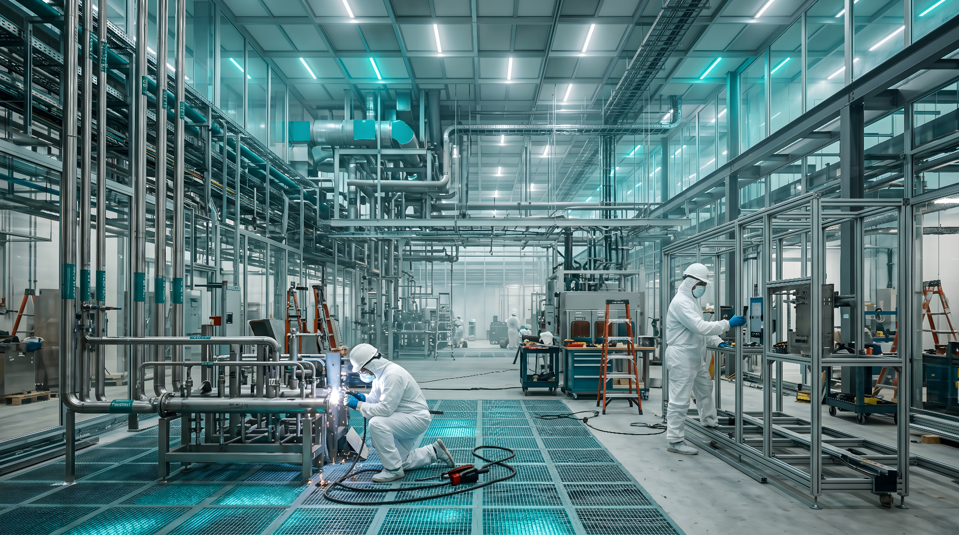
    LOD 350+ MEP coordination for ultra-pure water, gas, exhaust, and process chemical systems

    Deliverable 04

    Tool install pre-scanning and as-installed verification

    Deliverable 05

    Cleanroom-ready CAD and BIM deliverables in fab-standard formats

    Custom scope

    Need something not on this list? We custom-scope it.

    Discuss your scope
    Sector expertise

    Specialized capabilities

    The technical edge cases that separate semiconductor & cleanroom scopes from generic AEC engagements.

    ISO Class 5 / Class 1000 cleanroom-compliant equipment and procedures

    Verified scope

    No-touch, no-vibration scanning protocols

    Verified scope

    Background-suppressed deliverables (no proprietary tooling visible)

    Verified scope

    NDA-cleared field crews

    Verified scope

    Coordination with EHS, facilities, and process integration teams

    Verified scope

    Plus the edge cases your facility will surface during scoping.

    Tell us about your scope
    BimCon Solutions logo

    Semiconductor & Cleanroom Capability Sheet

    Download a one-page PDF overview of our semiconductor & cleanroom capabilities, deliverables, and engagement model.

    Download Capability Sheet (PDF)

    Semiconductor & Cleanroom BIM & VDC Services — BimCon Solutions

    BimCon Solutions delivers BIM coordination, 3D laser scanning, and MEP detailing for semiconductor & cleanroom facilities. Contactless scanning protocols for active fabs. ISO cleanroom-compliant workflows.

    Dense sub-fab process piping with 50+ utility servicesTool hookup coordination on aggressive installation schedules3D Laser ScanningScan-to-BIMBIM Coordination & Clash Detection

    BimCon Solutions

    BIM · VDC · Reality Capture

    Location
    Sioux Falls, SD 57104 · Nationwide
    Request a Fab Scan Quote

    Have a fab scope to discuss?

    NDA-friendly. Cleanroom-trained crews. Quote within one business day.

    Request a Fab Scan Quote

    Response within one business day.

    Confidential · NDA-ready · Nationwide deployment